An operational amplifier, which is often called an op-amp, is a DC-coupled high-gain electronic voltage amplifier with differential inputs[1] and, usually, a single output. Typically the output of the op-amp is controlled either by negative feedback, which largely determines the magnitude of its output voltage gain, or by positive feedback, which facilitates regenerative gain and oscillation. High input impedance at the input terminals and low output impedance are important typical characteristics.
Op-amps are among the most widely used electronic devices today, being used in a vast array of consumer, industrial, and scientific devices. Many standard IC op-amps cost only a few cents in moderate production volume; however some integrated or hybrid operational amplifiers with special performance specifications may cost over $100 US in small quantities.
Modern designs are electronically more rugged than earlier implementations and some can sustain direct short-circuits on their outputs without damage.
The op-amp is one type of differential amplifier. Other types of differential amplifier include the fully differential amplifier (similar to the op-amp, but with 2 outputs), the instrumentation amplifier (usually built from 3 op-amps), the isolation amplifier (similar to the instrumentation amplifier, but which works fine with common-mode voltages that would destroy an ordinary op-amp), and negative feedback amplifier (usually built from 1 or more op-amps and a resistive feedback network).
Circuit notation

The circuit symbol for an op-amp is shown in Figure 1
where:
- V + : non-inverting input
- V − : inverting input
- Vout: output
- VS + : positive power supply
- VS − : negative power supply
The power supply pins (VS + and VS − ) can be labeled in different ways (See IC power supply pins). Despite different labeling, the function remains the same. Often these pins are left out of the diagram for clarity, and the power configuration is described or assumed from the circuit.
Ideal op-amps

Shown on the right is an example of an ideal operational amplifier. The main part in an amplifier is the dependent voltage source that increases in relation to the voltage drop across Rin, thus amplifying the voltage difference between V + and V − . Many uses have been found for operational amplifiers and an ideal op-amp seeks to characterize the physical phenomena that make op-amps useful.
V + and V − are not connected to the circuit within the op-amp because they power the dependent voltage source's circuit (not shown). These are notable, however, because they determine the maximum voltage the dependent voltage source can output.
For any input voltages the ideal op-amp has
- infinite open-loop gain,
- infinite bandwidth,
- infinite input impedances (resulting in zero input currents),
- zero offset voltage,
- infinite slew rate,
- zero output impedance, and
- zero noise.
Because of these properties, an op-amp can be modeled as a nullor.
History


1941: First (vacuum tube) op-amp
An op-amp, defined as a general-purpose, DC-coupled, high gain, inverting feedback amplifier, is first found in US Patent 2,401,779 "Summing Amplifier" filed by Karl D. Swartzel Jr. of Bell labs in 1941. This design used three vacuum tubes to achieve a gain of 90dB and operated on voltage rails of ±350V. In contrast to modern day op-amps, it had a single inverting input and an output instead of the modern two differential inputs where one is inverting and the other is not. Throughout World War II, Swartzel's design proved its value by being liberally used in the M9 artillery director designed at Bell Labs. This artillery director worked with the SCR584 radar system to achieve extraordinary hit rates (near 90%) that would not have been possible otherwise.[2]
1947: First op-amp with an explicit non-inverting input
In 1947, the operational amplifier was first formally defined and named in a paper by Professor John R. Ragazzini of Columbia University. In this same paper a footnote mentioned an op-amp design by a student that would turn out to be quite significant. This op-amp, designed by Loebe Julie, was superior in a variety of ways. It had two major innovations. Its input stage used a long-tailed triode pair with loads matched to reduce drift in the output and, far more importantly, it was the first op-amp design to have two inputs (one inverting, the other non-inverting). The differential input made a whole range of new functionality possible, but it would not be used for a long time due to the rise of the chopper-stabilized amplifier.[3]
1948: First chopper-stabilized op-amp
In 1949, Edwin A. Goldberg designed a chopper-stabilized op-amp. This set-up uses a normal op-amp with an additional AC amplifier that goes alongside the op-amp. The chopper gets an AC signal from DC by switching between the DC voltage and ground at a fast rate (60Hz or 400Hz). This signal is then amplified, rectified, filtered and fed into the op-amp's non-inverting input. This vastly improved the gain of the op-amp while significantly reducing the output drift and DC offset. Unfortunately, any design that used a chopper couldn't use their non-inverting input for any other purpose. Nevertheless, the much improved characteristics of the chopper-stabilized op-amp made it the dominant way to use op-amps. Techniques that used the non-inverting input regularly would not be very popular until the 1960s when op-amp ICs started to show up in the field.
In 1953, vacuum tube op-amps became commercially available with the release of the K2-W from GAP/R. It sold in an octal package and had a (K2-P) chopper add-on available that would effectively "use up" the non-inverting input. This op-amp was based on a descendant of Loebe Julie's 1947 design and, along with its successors, would start the widespread use of op-amps in industry.
1961: First discrete IC op-amps
With the birth of the transistor in 1947, and the silicon transistor in 1954, the concept of ICs became a reality. The introduction of the planar process in 1959 made transistors and ICs stable enough to be commercially useful. By 1961, solid-state, discrete op-amps were being produced. These op-amps were effectively small circuit boards with packages such as edge-connectors. They usually had hand-selected resistors in order to improve things such as voltage offset and drift. The P45 (1961) had a gain of 94dB and ran on ±15V rails. It was intended to deal with signals in the range of ±10V.
1962: First op-amps in potted modules
By 1962, several companies were producing modular potted packages that could be plugged into printed circuit boards. These packages were crucially important as they made the operational amplifier into a single black box which could be easily treated as a component in a larger circuit.
1963: First monolithic IC op-amp
In 1963, the first monolithic IC op-amp, the μA702 designed by Bob Widlar at Fairchild Semiconductor, was released. Monolithic ICs consist of a single chip as opposed to a chip and discrete parts (a discrete IC) or multiple chips bonded and connected on a circuit board (a hybrid IC). Almost all modern op-amps are monolithic ICs; however, this first IC did not meet with much success. Issues such as an uneven supply voltage, low gain and a small dynamic range held off the dominance of monolithic op-amps until 1965 when the μA709[4] (also designed by Bob Widlar) was released.
1968: Release of the μA741 — would be seen as a nearly ubiquitous chip
The popularity of monolithic op-amps was further improved upon the release of the LM101 in 1967, which solved a variety of issues, and the subsequent release of the μA741 in 1968. The μA741 was extremely similar to the LM101 except that Fairchild's facilities allowed them to include a 30pF compensation capacitor inside the chip instead of requiring external compensation. This simple difference has made the 741 the canonical op-amp and many modern amps base their pinout on the 741's.The μA741 is still in production, and has become ubiquitous in electronics — many manufacturers produce a version of this classic chip, recognizable by part numbers containing "741."
1966: First varactor bridge op-amps
Since the 741, there have been many different directions taken in op-amp design. Varactor bridge op-amps started to be produced in the late 1960s; they were designed to have extremely small input current and are still amongst the best op-amps available in terms of common-mode rejection with the ability to correctly deal with 100s of Volts at its inputs.
1970: First high-speed, low-input current FET design
In the 1970s high speed, low-input current designs started to be made by using FETs. These would be largely replaced by op-amps made with MOSFETs in the 1980s. During the 1970s single sided supply op-amps also became available.
1972: Single sided supply op-amps being produced
The LM324 (released in 1972) was one such op-amp that came in a quad package and became an industry standard. In addition to packaging multiple op-amps in a single package, the 1970s also saw the birth of op-amps in hybrid packages. These op-amps were generally improved versions of existing monolithic op-amps and were without a doubt the best op-amps available. As the properties of monolithic op-amps improved, the more complex hybrid ICs were quickly relegated to systems that are required to have extremely long service lives or other specialty systems.
Applications
Use in electronics system design
The use of op-amps as circuit blocks is much easier and clearer than specifying all their individual circuit elements (transistors, resistors, etc.), whether the amplifiers used are integrated or discrete. In the first approximation op-amps can be used as if they were ideal differential gain blocks; at a later stage limits can be placed on the acceptable range of parameters for each op-amp.
Circuit design follows the same lines for all electronic circuits. A specification is drawn up governing what the circuit is required to do, with allowable limits. For example, the gain may be required to be 100 times, with a tolerance of 5% but drift of less than 1% in a specified temperature range; the input impedance not less than 1 megohm; etc.
A basic circuit is designed, often with the help of circuit modeling (on a computer). Specific commercially available op-amps and other components are then chosen that meet the design criteria within the specified tolerances at acceptable cost. If not all criteria can be met, the specification may need to be modified.
A prototype is then built and tested; changes to meet or improve the specification, alter functionality, or reduce the cost, may be made.
Method of application
The amplifier's differential inputs consist of V + input and a V − input, and generally the op-amp amplifies only the difference in voltage between the two. This is called the "differential input voltage". Operational amplifiers are usually used with feedback loops where the output of the amplifier would influence one of its inputs. The output voltage and the input voltage it influences settles down to a stable voltage after being connected for some time, when they satisfy the internal circuit of the op amp.
In its most common use, the op-amp's output voltage is controlled by feeding a fraction of the output signal back to the inverting input. This is known as negative feedback. If that fraction is zero, i.e., there is no negative feedback, the amplifier is said to be running "open loop" and its output is the differential input voltage multiplied by the total gain of the amplifier, as shown by the following equation:

where V + is the voltage at the non-inverting terminal, V − is the voltage at the inverting terminal and G is the total open-loop gain of the amplifier.
Because the magnitude of the open-loop gain is typically very large and not well controlled by the manufacturing process, op-amps are not usually used without negative feedback. Unless the differential input voltage is extremely small, open-loop operation results in op-amp saturation (see below in Nonlinear imperfections). An example of how the output voltage is calculated when negative feedback exists is shown below in Basic non-inverting amplifier circuit.
Another typical configuration of op-amps is the positive feedback, which takes a fraction of the output signal back to the non-inverting input. An important application of it is the comparator with hysteresis (see Schmitt trigger).
Basic non-inverting amplifier circuit
The general op-amp has two inputs and one output. The output voltage is a multiple of the difference between the two inputs (some are made with floating, differential outputs):
G is the open-loop gain of the op-amp. The inputs are assumed to have very high impedance; negligible current will flow into or out of the inputs. Op-amp outputs have very low source impedance.
If the output is connected to the inverting input, after being scaled by a voltage divider:
then:
- V + = Vin


Solving for Vout / Vin, we see that the result is a linear amplifier with gain:

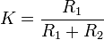
If G is very large, Vout / Vin comes close to 1 / K, which equals 1 + (R2 / R1).
This negative feedback connection is the most typical use of an op-amp, but many different configurations are possible, making it one of the most versatile of all electronic building blocks.
When connected in a negative feedback configuration, the op-amp will try to make Vout whatever voltage is necessary to make the input voltages as nearly equal as possible. This, and the high input impedance, are sometimes called the two "golden rules" of op-amp design for circuits that use negative feedback:
- No current will flow into the inputs.
- The input voltages will be nearly equal.
The exception is if the voltage required is greater than the op-amp's supply, in which case the output signal stops near the power supply rails, VS + or VS − .
Most single, dual and quad op-amps available have a standardized pin-out which permits one type to be substituted for another without wiring changes. A specific op-amp may be chosen for its open loop gain, bandwidth, noise performance, input impedance, power consumption, or a compromise between any of these factors.
Other applications
- audio- and video-frequency pre-amplifiers and buffers
- voltage comparators
- differential amplifiers
- differentiators and integrators
- filters
- precision rectifiers
- precision peak detectors
- voltage and current regulators
- analog calculators
- analog-to-digital converters
- digital-to-analog converter
- voltage clamps
- oscillators and waveform generators
Limitations of real op-amps
Real op-amps can only approach this ideal: in addition to the practical limitations on slew rate, bandwidth, offset and so forth mentioned above, real op-amp parameters are subject to drift over time and with changes in temperature, input conditions, etc. Modern integrated FET or MOSFET op-amps approximate more closely the ideal op-amp than bipolar ICs where large signals must be handled at room temperature over a limited bandwidth; input impedance, in particular, is much higher, although the bipolar op-amps usually exhibit superior (i.e., lower) input offset drift and noise characteristics.
Where the limitations of real devices can be ignored, an op-amp can be viewed as a black box with gain; circuit function and parameters are determined by feedback, usually negative. IC op-amps as implemented in practice are moderately complex integrated circuits; see the internal circuitry for the relatively simple 741 op-amp below, for example.
DC imperfections
Real operational amplifiers suffer from several non-ideal effects:
- Finite gain — Open-loop gain is defined as the amplification from input to output without any feedback applied. For mathematical calculations, the ideal open-loop gain is infinite; however, it is finite in real operational amplifiers. Typical devices exhibit open-loop DC gain ranging from 100,000 to over 1 million. So long as the loop gain (i.e., the product of open-loop and feedback gains) is very large, the circuit gain will be determined entirely by the amount of negative feedback (i.e., it will be independent of open-loop gain). In cases where closed-loop gain must be very high, the feedback gain will be very low, and the low feedback gain causes low loop gain; in these cases, the operational amplifier will cease to behave ideally.
- Finite input impedance — The input impedance of the operational amplifier is defined as the impedance between its two inputs. It is not the impedance from each input to ground. In the typical high-gain negative-feedback applications, the feedback ensures that the two inputs sit at the same voltage, and so the impedance between them is made artificially very high. Hence, this parameter is rarely an important design parameter. Because MOSFET-input operational amplifiers often have protection circuits that effectively short circuit any input differences greater than a small threshold, the input impedance can appear to be very low in some tests. However, as long as these operational amplifiers are used in a typical high-gain negative feedback application, these protection circuits will be inactive and the negative feedback will render the input impedance to be practically infinite. The input bias and leakage currents described below are a more important design parameter for typical operational amplifier applications.
- Nonzero output impedance — Low output impedance is important for low resistance loads; for these loads, the voltage drop across the output impedance of the amplifier will be significant. Hence, the output impedance of the amplifier reflects the maximum power that can be provided. Similarly, low-impedance outputs typically require high quiescent (i.e., "idle") current in the output stage and will dissipate more power. So low-power designs may purposely sacrifice low-impedance outputs.
- Input current — Due to biasing requirements or leakage, a small amount of current (typically ~10 nanoAmperes (nA) for bipolar op-amps, tens of picoAmperes (pA) for JFET input stages, and only a few pA for MOSFET input stages) flows into the inputs. When large resistors or sources with high output impedances are used in the circuit, these small currents can produce large unmodeled voltages. If the input currents are matched and the impedance looking out of both inputs are matched, then the voltages produced at each input will be equal. Because the operational amplifier operates on the difference between its inputs, these matched voltages will have no effect (unless the operational amplifier has poor CMRR, which is described below). It is more common for the input currents (or the impedances looking out of each input) to be slightly mismatched, and so a small offset voltage can be produced. This offset voltage can create offsets or drifting in the operational amplifier. It can often be nulled externally; however, many operational amplifiers include offset null or balance pins and some procedure for using them to remove this offset. Some operational amplifiers attempt to nullify this offset automatically.
- Input offset voltage — This voltage, which is what is required across the op-amp's input terminals to drive the output voltage to zero[5], is related to the mismatches in input bias current. In the perfect amplifier, there would be no input offset voltage. However, it exists in actual op-amps because of imperfections in the differential amplifier that constitutes the input stage of the vast majority of these devices. Input offset voltage creates two problems: First, due to the amplifier's high voltage gain, it virtually assures that the amplifier output will go into saturation if it is operated without negative feedback, even when the input terminals are wired together. Second, in a closed loop, negative feedback configuration, the input offset voltage is amplified along with the signal and this may pose a problem if high precision DC amplification is required or if the input signal is very small.[6]
- Common mode gain — A perfect operational amplifier amplifies only the voltage difference between its two inputs, completely rejecting all voltages that are common to both. However, the differential input stage of an operational amplifier is never perfect, leading to the amplification of these identical voltages to some degree. The standard measure of this defect is called the common-mode rejection ratio (denoted, CMRR). Minimization of common mode gain is usually important in non-inverting amplifiers (described below) that operate at high amplification.
- Temperature effects — All parameters change with temperature. Temperature drift of the input offset voltage is especially important.
- Power-supply rejection — The output of a perfect operational amplifier will be completely independent from ripples that arrive on its power supply inputs. Every real operational amplifier has a specified power supply rejection ratios (PSRR) that reflects how well the op-amp can reject changes in its supply voltage. Copious use of bypass capacitors can improve the PSRR of many devices, including the operational amplifier.
AC imperfections
The op-amp gain calculated at DC does not apply at higher frequencies. To a first approximation, the gain of a typical op-amp is inversely proportional to frequency. This means that an op-amp is characterized by its gain-bandwidth product. For example, an op-amp with a gain bandwidth product of 1 MHz would have a gain of 5 at 200 kHz, and a gain of 1 at 1 MHz. This low-pass characteristic is introduced deliberately, because it tends to stabilize the circuit by introducing a dominant pole. This is known as frequency compensation.
Typical low cost, general purpose op-amps exhibit a gain bandwidth product of a few megahertz. Specialty and high speed op-amps can achieve gain bandwidth products of hundreds of megahertz. For very high-frequency circuits, a completely different form of op-amp called the current-feedback operational amplifier is often used.
Other imperfections include:
- Finite bandwidth — all amplifiers have a finite bandwidth. This creates several problems for op amps. First, associated with the bandwidth limitation is a phase difference between the input signal and the amplifier output that can lead to oscillation in some feedback circuits. The internal frequency compensation used in some op amps to increase the gain or phase margin intentionally reduces the bandwidth even further to maintain output stability when using a wide variety of feedback networks. Second, reduced bandwidth results in lower amounts of feedback at higher frequencies, producing higher distortion, noise, and output impedance and also reduced output phase linearity as the frequency increases.
- Input capacitance — most important for high frequency operation because it further reduces the open loop bandwidth of the amplifier.
- Common mode gain — See DC imperfections, above.
Nonlinear imperfections
- Saturation — output voltage is limited to a minimum and maximum value close to the power supply voltages.[7] Saturation occurs when the output of the amplifier reaches this value and is usually due to:
- In the case of an op-amp using a bipolar power supply, a voltage gain that produces an output that is more positive or more negative than that maximum or minimum; or
- In the case of an op-amp using a single supply voltage, either a voltage gain that produces an output that is more positive than that maximum, or a signal so close to ground that the amplifier's gain is not sufficient to raise it above the lower threshold.[8]
- Slewing — the amplifier's output voltage reaches its maximum rate of change. Measured as the slew rate, it is usually specified in volts per microsecond. When slewing occurs, further increases in the input signal have no effect on the rate of change of the output. Slewing is usually caused by internal capacitances in the amplifier, especially those used to implement its frequency compensation.
- Non-linear transfer function — The output voltage may not be accurately proportional to the difference between the input voltages. It is commonly called distortion when the input signal is a waveform. This effect will be very small in a practical circuit if substantial negative feedback is used.
Distortion in op-amps
Very often operational amplifiers are used for audio filters. It is important to evaluate the distortion introduced by the Distortion Multiplication Factor (Kd) described by Oscar Bonello [9] The behavior of this type of operational amplifiers is important to get low distortion amplifiers and audio consoles for sound recording and reproduction.
Power considerations
- Limited output current — the output current must obviously be finite. In practice, most op-amps are designed to limit the output current so as not to exceed a specified level — around 25 mA for a type 741 IC op-amp — thus protecting the op-amp and associated circuitry from damage.
- Limited dissipated power — an opamp is a linear amplifier. It therefore dissipates some power as heat, proportional to the output current, and to the difference between the output voltage and the supply voltage. If the opamp dissipates too much power, then its temperature will increase above some safe limit. The opamp may enter thermal shutdown, or it may be destroyed.
Internal circuitry of 741 type op-amp

Though designs vary between products and manufacturers, all op-amps have basically the same internal structure, which consists of three stages:
- Differential amplifier
- Input stage — provides low noise amplification, high input impedance, usually a differential output
- Voltage amplifier
- Provides high voltage gain, a single-pole frequency roll-off, usually single-ended output
- Output amplifier
- Output stage — provides high current driving capability, low output impedance, current limiting and short circuit protection circuitry
Current mirrors
The sections outlined in red are current mirrors. The primary current, from which other standing (bias) currents are generated, is determined by the chip's power supply and the 39 kΩ resistor acting (with the two transistor diode junctions) as a current source. The current generated is approximately (VS + − VS − − 2Vbe) / 39 kΩ. The input stage DC conditions are controlled by the two current mirrors on the left. Q10 and Q11 form a Widlar current source where the 5 kΩ resistor sets the collector current of Q10 to a very small fraction of the primary current. The constant Q10 current supplies the base current for Q3 and Q4 but must also supply the Q9 collector current, which the Q8/Q9 current mirror will try to make as large as the Q3 and Q4 collector currents. Thus the Q3/Q4 base current (which is of the same order as the input currents) will be a small fraction of the already small Q10 current. Another way of looking at this is that if the input stage current tends to increase above the Q10 current, the Q8/Q9 current mirror will draw current away from the common base of Q3 and Q4, throttling the input stage, and vice versa. Thus the input stage DC conditions are stabilized by a high-gain negative feedback system. The feedback loop also isolates the rest of the circuit from common mode variations by making the base voltage of Q3/Q4 follow tightly 2Vbe below that of the highest input voltage.
The top-right current mirror Q12/Q13 provides a constant current load for the class A gain stage, via the collector of Q13, that is largely independent of the output voltage.
Differential input stage
The blue outlined section is a differential amplifier. Q1 and Q2 are input emitter followers and together with the common base pair Q3 and Q4 form the differential input stage. In addition, Q3 and Q4 also act as level shifters and provide voltage gain to drive the class A amplifier. They also help to increase the reverse Vbe rating on the input transistors.
The differential amplifier formed by Q1 - Q4 drives a current mirror active load formed by transistors Q5 - Q7. Q7 increases the accuracy of the current mirror by decreasing the amount of signal current required from Q3 to drive the bases of Q5 and Q6. This current mirror provides differential to single ended conversion as follows:
The signal current of Q3 is the input to the current mirror while the output of the mirror (the collector of Q6) is connected to the collector of Q4. Here, the signal currents of Q3 and Q4 are summed. For differential input signals, the signal currents of Q3 and Q4 are equal and opposite. Thus, the sum is twice the individual signal currents. This completes the differential to single ended conversion.
The open circuit signal voltage appearing at this point is given by the product of the summed signal currents and the paralleled collector resistances of Q4 and Q6. Since the collectors of Q4 and Q6 appear as high resistances to the signal current, the open circuit voltage gain of this stage is very high.
It should be noted that the base current at the inputs is not zero and the effective (differential) input impedance of a 741 is about 2 MΩ. The "offset null" pins may be used to place external resistors in parallel with the two 1 kΩ resistors (typically in the form of the two ends of a potentiometer) to adjust the balancing of the Q5/Q6 current mirror and thus indirectly control the output of the op-amp when zero signal is applied between the inputs.
Class A gain stage
The section outlined in magenta is the class A gain stage. It consists of two NPN transistors in a Darlington configuration and uses the output side of a current mirror as its collector load to achieve high gain. The 30 pF capacitor provides frequency selective negative feedback around the class A gain stage as a means of frequency compensation to stabilise the amplifier in feedback configurations. This technique is called Miller compensation and functions in a similar manner to an op-amp integrator circuit. It is also known as 'dominant pole compensation' because it introduces a dominant pole (one which masks the effects of other poles) into the open loop frequency response. This pole can be as low as 10 Hz in a 741 amplifier and it introduces a −3 dB loss into the open loop response at this frequency. This is done to achieve unconditional stability of the amplifier down to unity closed loop gain using non-reactive feedback networks and makes this type of internally compensated amplifier easier to use.
Output bias circuitry
The green outlined section (based around Q16) is a voltage level shifter or rubber diode (i.e., a VBE multiplier); a type of voltage source. In the circuit as shown, Q16 provides a constant voltage drop between its collector and emitter regardless of the current through the circuit. If the base current to the transistor is assumed to be zero, and the voltage between base and emitter (and across the 7.5 kΩ resistor) is 0.625 V (a typical value for a BJT in the active region), then the current through the 4.5 kΩ resistor will be the same as that through the 7.5 kΩ, and will produce a voltage of 0.375 V across it. This keeps the voltage across the transistor, and the two resistors at 0.625 + 0.375 = 1 V. This serves to bias the two output transistors slightly into conduction reducing crossover distortion. In some discrete component amplifiers this function is achieved with (usually two) silicon diodes.
Output stage
The output stage (outlined in cyan) is a Class AB push-pull emitter follower (Q14, Q20) amplifier with the bias set by the Vbe multiplier voltage source Q16 and its base resistors. This stage is effectively driven by the collectors of Q13 and Q19. The output range of the amplifier is about 1 volt less than the supply voltage, owing in part to Vbe of the output transistors Q14 and Q20.
The 25 Ω resistor in the output stage acts as a current sense to provide the output current-limiting function which limits the current in the emitter follower Q14 to about 25 mA for the 741. Current limiting for the negative output is done by sensing the voltage across Q19's emitter resistor and using this to reduce the drive into Q15's base. Later versions of this amplifier schematic may show a slightly different method of output current limiting. The output resistance is not zero as it would be in an ideal op-amp but with negative feedback it approaches zero.
Note: while the 741 was historically used in audio and other sensitive equipment, such use is now rare because of the improved noise performance of more modern op-amps. Apart from generating noticeable hiss, 741s and other older op-amps may have poor common-mode rejection ratios and so will often introduce cable-borne mains hum and other common-mode interference, such as switch 'clicks', into sensitive equipment.


No comments:
Post a Comment